

 Robert
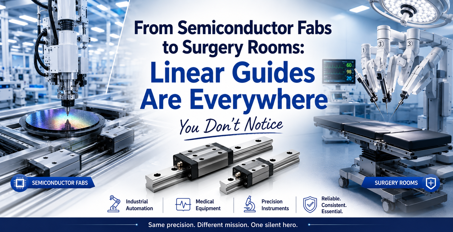
From Semiconductor Fabs to Surgery Rooms: Linear Guides Are Everywhere You Don't Notice
$8.2B Global Market (2024) 6.4% CAGR Through 2030 20+ Industries Served The Invisible Infrastructure of Modern Manufacturing Think...
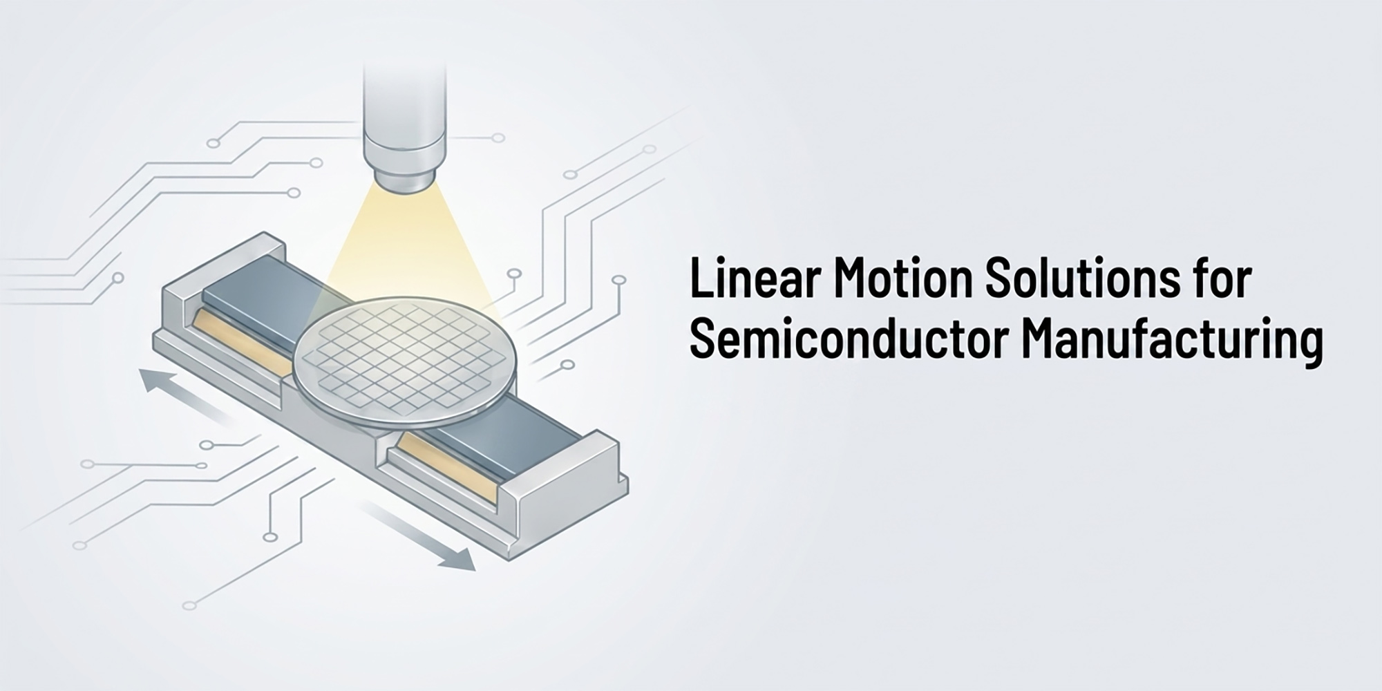
Table of Contents
The semiconductor industry stands at the forefront of technological innovation, demanding unprecedented levels of precision, cleanliness, and reliability. At the heart of semiconductor manufacturing processes lies a critical yet often overlooked component: linear motion systems. These sophisticated solutions enable the nanometer-level accuracy required for modern chip fabrication, wafer handling, and inspection processes.
As semiconductor devices continue to shrink in size while increasing in complexity, the role of high-precision linear motion solutions becomes increasingly vital. From wafer steppers that position substrates with sub-micron accuracy to pick-and-place systems that handle delicate silicon wafers, linear motion technology serves as the backbone of semiconductor production.
Modern semiconductor fabrication is perhaps the most precision-demanding manufacturing process in human history. At the heart of every wafer scanner, wire bonder, and die sorter lies an unsung hero: the linear motion system.
Semiconductor chips now routinely feature transistor nodes below 3 nm — a scale so small that a single human hair is roughly 30,000 times wider. To achieve this, the equipment that positions, exposes, etches, and inspects wafers must repeat movements with nanometer-level accuracy, thousands of times per hour, day after day, without failure.
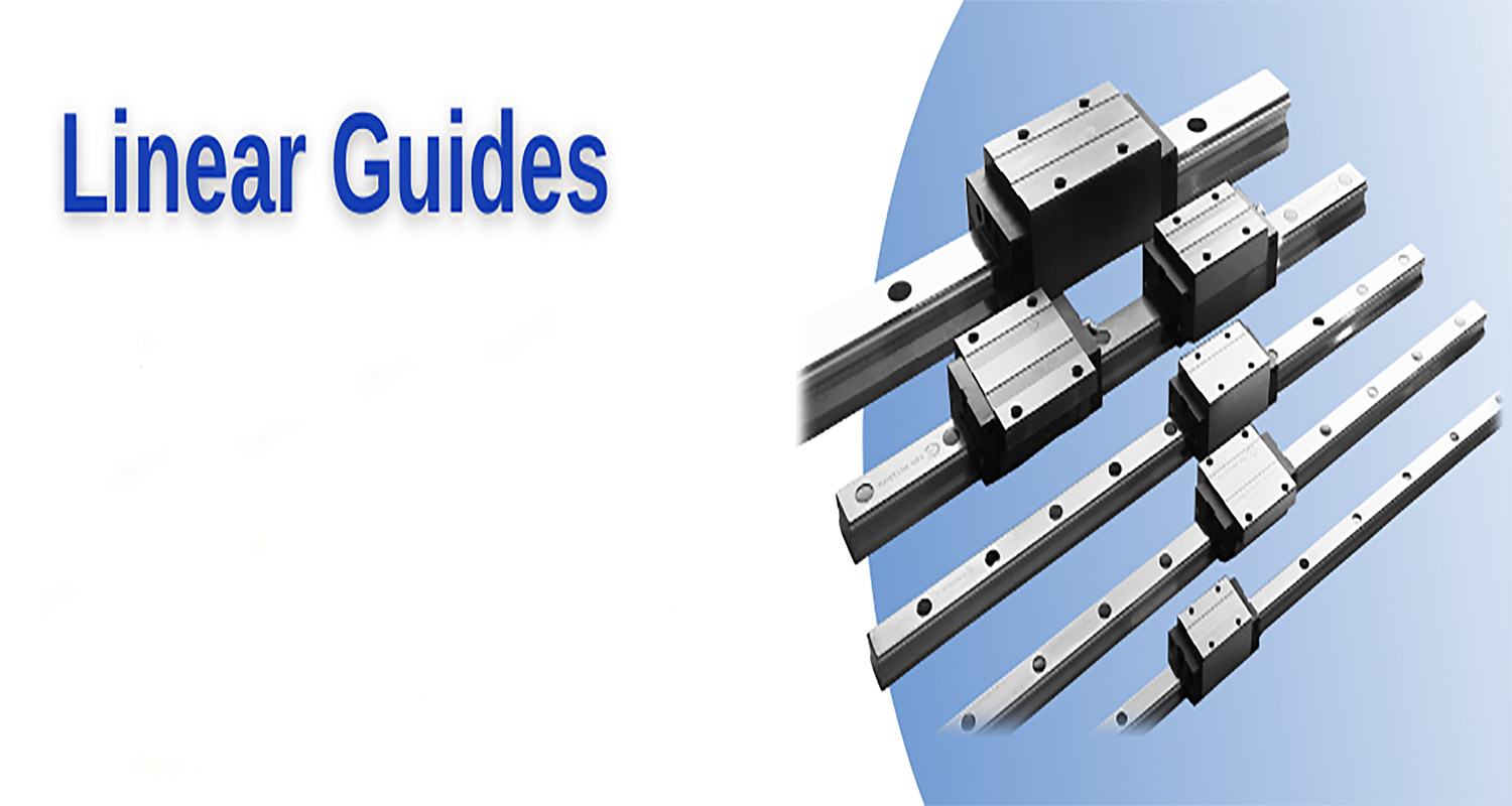
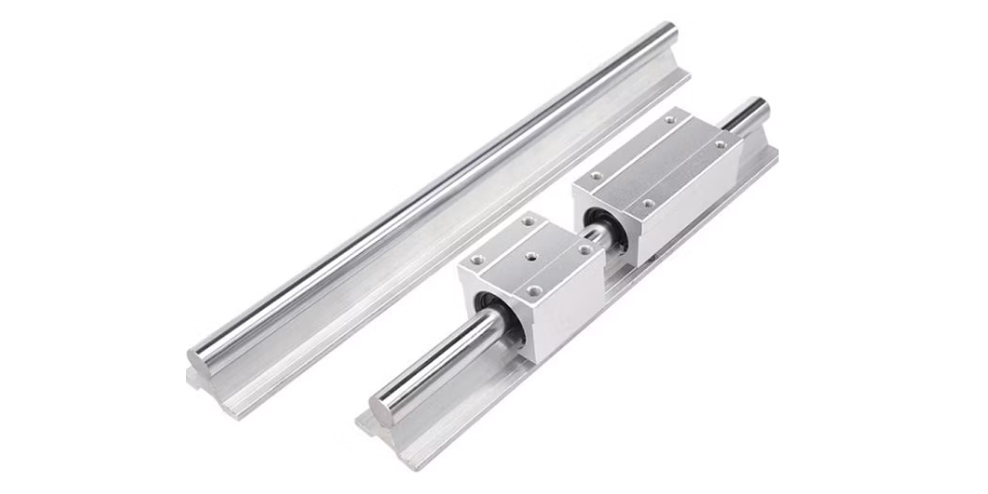
Linear guides — also called linear rails, linear slideways, or linear motion guides — provide the controlled, one-dimensional movement that makes this possible. Whether it is the gantry of a lithography scanner aligning a reticle over a 300 mm silicon wafer, or a robotic arm transferring fragile substrates between process chambers, linear guides are the mechanical foundation underpinning every move.
|
±1 nm |
$600B+ |
1M+ |
3 nm |
|
Positioning repeatability in advanced lithography |
Global semiconductor equipment market by 2030 |
Wafer moves per tool per year in a high-volume fab |
Leading-edge node size requiring atomic-scale positioning |
The global market for semiconductor manufacturing equipment exceeded $100 billion in 2023, and continues to grow as demand for AI processors, memory chips, and power devices accelerates. Every new fab built — from Taiwan to Arizona to Saxony — represents billions of dollars in capital equipment investment, all of which depends on linear motion systems that perform reliably in cleanroom conditions.
Semiconductor fabs deploy several fundamentally different types of linear motion systems, each optimized for different combinations of speed, precision, load capacity, and cleanliness requirements.
|
System Type |
Contact Method |
Speed Capability |
Key Advantage |
Primary Use Case |
|
Recirculating Ball Guide |
Point contact |
Up to 5 m/s |
Low friction, wide availability |
Wafer handlers, general automation |
|
Roller Linear Guide |
Line contact |
Up to 3 m/s |
High stiffness, large load capacity |
Process modules, heavy stages |
|
Air Bearing Stage |
Non-contact |
Up to 2 m/s |
Zero wear, nanometer precision |
Lithography scanners, metrology |
|
Magnetic Levitation |
Non-contact |
Up to 2+ m/s |
Particle-free, contactless |
Next-gen EUV, advanced R&D |
|
Profile Rail (4-row) |
Point/line contact |
Up to 4 m/s |
High moment load capacity |
Multi-axis wafer handling |
|
Crossed Roller Guide |
Line contact |
Up to 1 m/s |
Maximum rigidity, compact |
Probe stages, inspection tools |
Table 1: Linear motion system types and characteristics for semiconductor applications
The choice between ball and roller recirculating elements defines the foundational trade-off in most fab equipment. Ball elements offer lower friction and better high-speed performance but carry loads through point contact, limiting capacity per unit size.
Roller elements provide line contact, dramatically increasing load and moment capacity and stiffness — at the cost of slightly higher friction and running noise. For heavy process modules of CVD, PVD, and etch tools, roller guides are often preferred. For high-throughput wafer transport robots, ball guides dominate.
Linear guides in semiconductor fabs must satisfy a cluster of demanding requirements simultaneously — a combination not found in any other manufacturing environment. Understanding these requirements is the starting point for any selection or specification exercise.
|
Requirement |
Typical Specification |
Impact If Not Met |
|
Positioning Accuracy |
≤±1 µm (ball screw stages); ≤±1 nm (air bearing lithography) |
Overlay errors, CD variation, yield loss |
|
Repeatability |
≤0.1 µm bidirectional |
Process drift, wafer-to-wafer non-uniformity |
|
Running Parallelism |
≤2 µm/300 mm stroke |
Wafer tilt, focus errors in lithography |
|
Particle Generation |
Class 1 cleanroom compatible (ISO 3) |
Wafer contamination, defect density increase |
|
Outgassing |
<10⁻⁸ Pa·m³/s (vacuum-rated) |
Vacuum level degradation, film contamination |
|
Speed |
1–5 m/s (wafer handlers); up to 10 m/s (sort/test) |
Throughput loss, reduced UPH |
|
Acceleration |
2–50 m/s² depending on stage type |
Slower move-and-settle, lower wafers/hour |
|
Service Life |
5–10 years / 10,000+ km travel |
Unplanned downtime, costly field replacement |
|
Corrosion Resistance |
Stainless steel or ceramic |
Guide degradation, metallic contamination |
|
Magnetic Compatibility |
Non-magnetic materials required |
Interference with e-beam, ion implant tools |
Table 2: Key performance requirements for linear guides in semiconductor manufacturing equipment
|
⚙ Cleanroom Compatibility Is Non-Negotiable. Unlike industrial or automotive applications, semiconductor fabs operate under ISO Class 3–5 cleanroom conditions (ISO 14644-1). Any linear motion component used in or near process equipment must be validated for low particle emission, zero silicone contamination, and compatibility with cleanroom-approved lubricants. |
Lithography is the most motion-intensive step in chip fabrication. In an EUV scanner, the wafer stage moves at speeds of up to 2 m/s while maintaining overlay accuracy of just ±1.5 nm. The reticle stage above it moves simultaneously in the opposite direction. Both are levitated by precisely controlled air bearings — the most sophisticated linear motion technology in commercial use.
Atmospheric and vacuum wafer handling robots use linear guide modules for the Z-axis (vertical) and radial extension axes. These guides must combine cleanroom compatibility with high cycle life — 10+ million cycles over tool lifetime — smooth low-friction motion to prevent wafer slip, and corrosion resistance against atmospheric moisture and process chemical exposure.
Electrical test equipment places probes on individual die contacts at room temperature and at temperature extremes (−40°C to +200°C). The XY chuck stage must deliver sub-micron step precision at high throughput — up to 10,000 die touchdowns per hour on memory devices. Crossed roller guides or high-precision ball rail guides with preloaded carriages and zero-backlash ball screws are essential.
CMP tools use linear guides to control the down-force head and conditioning disk actuators. These operate in a wet, chemically aggressive environment with abrasive slurries. Corrosion-resistant 316L stainless steel or ceramic-element guides with sealed carriages and chemically compatible seals are required.
Backend packaging equipment moves at extreme speeds — wire bonders loop gold or copper wire at up to 25 bonds per second. The XY table beneath the bonding head must have ultralow-friction guides, near-zero stick-slip, and sub-micron repeatability. Miniature linear guides with ceramic ball elements are preferred.
|
Technology |
Accuracy Class |
Speed Capability |
Load Capacity |
Cleanroom Grade |
Typical Application |
|
Profile Rail (Ball) |
UP to SP class (±0.5 µm) |
Up to 5 m/s |
Medium–High |
Clean (certified grease) |
Wafer handlers, automation |
|
Profile Rail (Roller) |
SP to HP class |
Up to 3 m/s |
Very High |
Clean (sealed option) |
Process chamber support |
|
Crossed Roller Guide |
High precision (<0.5 µm) |
Low–Medium (≤1 m/s) |
Medium |
Excellent |
Probers, metrology |
|
Air Bearing Stage |
Nanometer (<5 nm) |
Up to 2 m/s |
Low–Medium |
Excellent (no lubricant) |
Lithography, interferometry |
|
Magnetic Levitation |
Sub-nanometer |
Up to 2+ m/s |
Medium |
Excellent (contactless) |
Next-gen EUV, advanced R&D |
|
Miniature Ball Guide |
Precision (±1–2 µm) |
Up to 10 m/s |
Low |
Good (ceramic ball option) |
Wire bonding, die attach |
Selecting a linear guide for semiconductor equipment is a multi-dimensional engineering decision. A structured selection process reduces risk and ensures the chosen system meets both performance and compliance requirements.
"The cost of a linear guide failure in a running fab is not the cost of the guide — it is the cost of the downtime, the scrapped wafers, and the engineering investigation that follows."
✓ Define the Motion Profile: Speed, acceleration, stroke, duty cycle, and settling time requirements. Use these to calculate required dynamic load rating and life expectancy.
✓ Quantify Loads: Include all forces — cutting, process, inertia, gravity. Calculate moment loads in all three planes (pitch, yaw, roll).
✓ Specify Accuracy Class: Semiconductor equipment typically requires Normal (N), High (H), Precision (P), Super Precision (SP), or Ultra Precision (UP) classes per ISO/JIS standards.
✓ Evaluate Environmental Conditions: Cleanroom class, temperature range, chemical exposure, humidity, and vacuum level all constrain material and lubrication choices.
✓ Confirm Preload Class: Choose preload (C0–C3) based on stiffness requirements. For most precision stages, light preload (C1–C2) is optimal.
✓ Select Lubrication Strategy: Cleanroom-certified fluorinated grease (PFPE-based) or dry film depending on vacuum and chemical requirements.
✓ Verify Material Compatibility: Stainless steel (440C) for corrosive environments; ceramic balls for non-magnetic and high-speed needs.
✓ Confirm Lead Time: Precision semiconductor-grade guides often have 12–20 week lead times. Build buffer stock for critical tools.
|
Application |
Recommended Guide Type |
Accuracy Class |
Special Requirements |
|
Atmospheric wafer handler |
Profile Rail (Ball, SS) |
SP or UP |
PFPE grease, cleaned & bagged |
|
Vacuum robot Z-axis |
Profile Rail (SS, sealed) |
P or SP |
Low outgassing grease or dry lube |
|
Wafer prober XY chuck |
Crossed Roller Guide |
UP |
Pre-loaded, zero backlash, temp-rated |
|
CMP down-force head |
Profile Rail (316L SS) |
H or P |
Chemical-resistant seals, IP65+ |
|
Wire bonder XY table |
Miniature Guide (ceramic ball) |
SP |
Non-magnetic, ultra-low friction |
|
Inspection/metrology stage |
Air Bearing Stage |
Nanometer |
Clean dry air, granite surface |
Table 4: Application-based guide selection for semiconductor tools
Even the most precisely manufactured linear guide will fail prematurely if maintained improperly. In semiconductor fabs, the stakes are especially high — a degraded guide does not just fail mechanically; it generates particles that contaminate wafers, and its degrading accuracy can cause subtle yield drift that is expensive to diagnose.
PFPE (perfluoropolyether) greases are the standard choice for cleanroom-rated guides: they are chemically inert, have extremely low vapor pressure, and generate minimal particles. Many suppliers offer integrated lube units (ILU) — small reservoirs mounted on the carriage that provide controlled metered lubrication over millions of cycles without manual intervention.
Cleanroom maintenance teams should periodically inspect guide seals for wear and verify carriage wiper integrity. Worn seals are a leading source of metallic particle contamination. High-cycle applications should plan seal replacement at scheduled PM intervals — typically every 12–18 months.
|
Maintenance Task |
Frequency |
Method |
Action Threshold |
|
Lubrication (PFPE grease) |
Per ILU schedule or every 6 months |
Integrated lube unit or syringe |
Increase in drive current or friction |
|
Seal and wiper inspection |
Quarterly or at PM |
Visual, tactile inspection |
Any visible wear, cracking, or contamination |
|
Parallelism measurement |
Bi-annual or after tool crash |
Laser interferometer |
>2 µm/300 mm deviation |
|
Running noise check |
Monthly |
Acoustic sensor or technician check |
Grinding, clicking, or irregular sound |
|
Full guide replacement |
Per life cycle spec |
OEM procedure |
End of rated travel life or particle events |
The long-anticipated move toward 450 mm wafer processing will require larger and stiffer linear guide systems for wafer handling, lithography, and process equipment. This places new demands on flatness, thermal stability, and load capacity of guide rail systems.
Leading motion component manufacturers are embedding sensors — vibration accelerometers, temperature probes, current monitors — directly in guide carriages to enable real-time condition monitoring. AI-driven analytics platforms process sensor data streams to forecast remaining useful life and flag anomalies before they cause failures.
As fabs push toward even lower contamination levels and increased vacuum integration, dry-lubricated linear guides with PTFE or DLC (diamond-like carbon) coatings are gaining adoption. These eliminate lubricant management entirely — no grease, no relubrication intervals, no volatile organics.
The convergence of ironless linear servo motors with precision profile rail guides is the dominant architecture for high-performance semiconductor stages today. The next evolution — fully integrated mechatronic modules with embedded motor, encoder, guide, and controller — will simplify fab equipment design and reduce alignment complexity.
Silicon carbide, zirconia, and alumina ceramic linear guides are seeing growing adoption in applications where zero magnetic interference, extreme chemical resistance, or ultra-low coefficient of thermal expansion are required.
Linear motion solutions are not peripheral components in semiconductor manufacturing — they are fundamental enablers of precision, throughput, and yield. Every nanometer of wafer positioning accuracy, every clean transfer of a fragile substrate, every reliable die attach bond ultimately traces back to the quality and suitability of the linear guides at the core of the equipment.
Selecting the right linear guide for semiconductor applications requires understanding both the mechanical demands — accuracy, stiffness, speed, life — and the environmental constraints: cleanliness, outgassing, chemical compatibility, magnetic neutrality.
No single guide type serves all applications. The best solution emerges from a disciplined engineering analysis matched to the specific tool, process, and cleanroom environment.
As the semiconductor industry continues its relentless march toward smaller nodes, larger wafers, and higher throughput, the demands on linear motion technology will only intensify. Engineers who understand these systems — from specification through selection, installation, and maintenance — will be essential contributors to the fabs that produce the chips powering our digital world.
$8.2B Global Market (2024) 6.4% CAGR Through 2030 20+ Industries Served The Invisible Infrastructure of Modern Manufacturing Think...
The Critical Role of Linear Motion Linear guide rails are crucial components for achieving precise, smooth motion in automation, robotics, and...
Linear guides are the backbone of precision motion in modern manufacturing, automation, and CNC machinery. When these critical components fail,...